Introduction
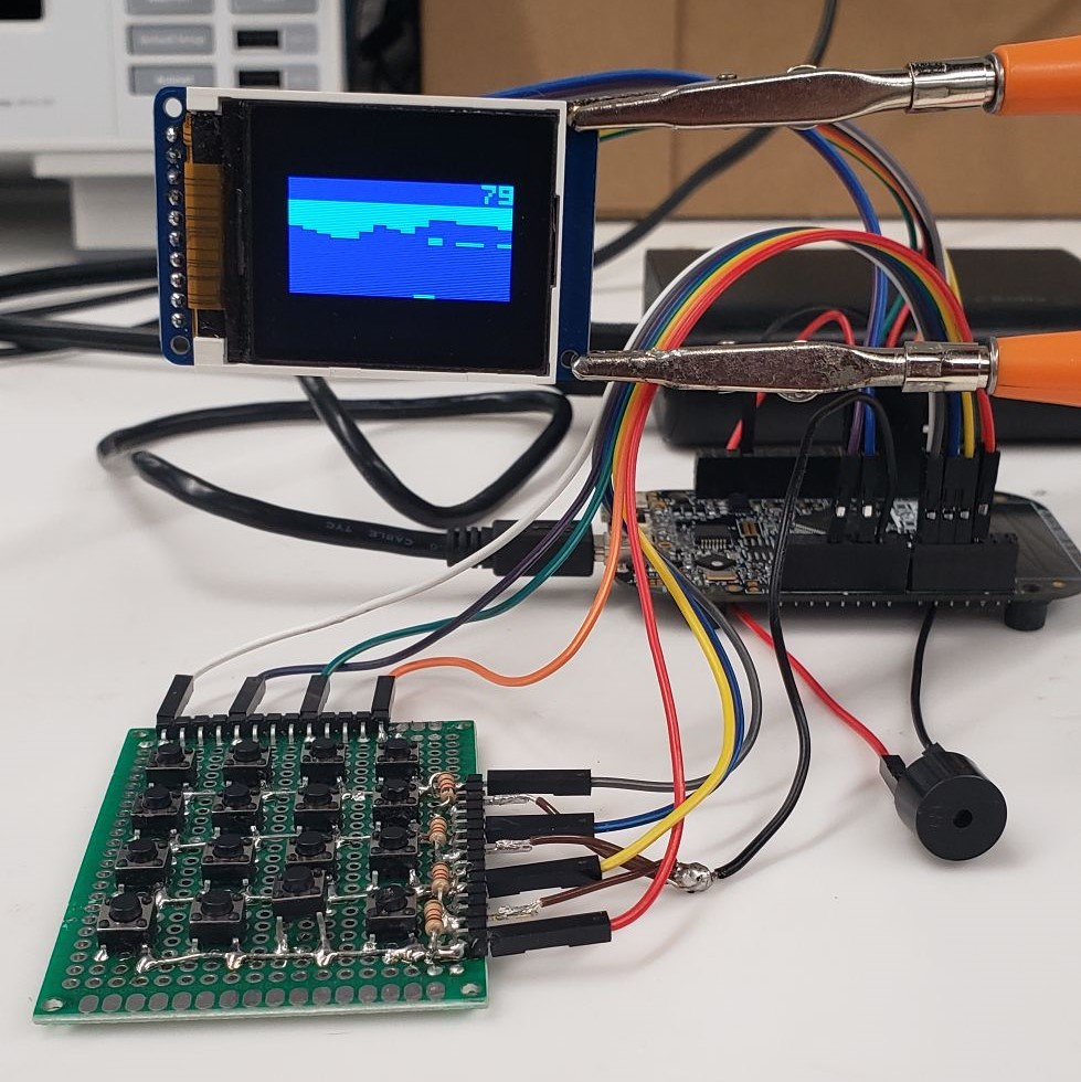
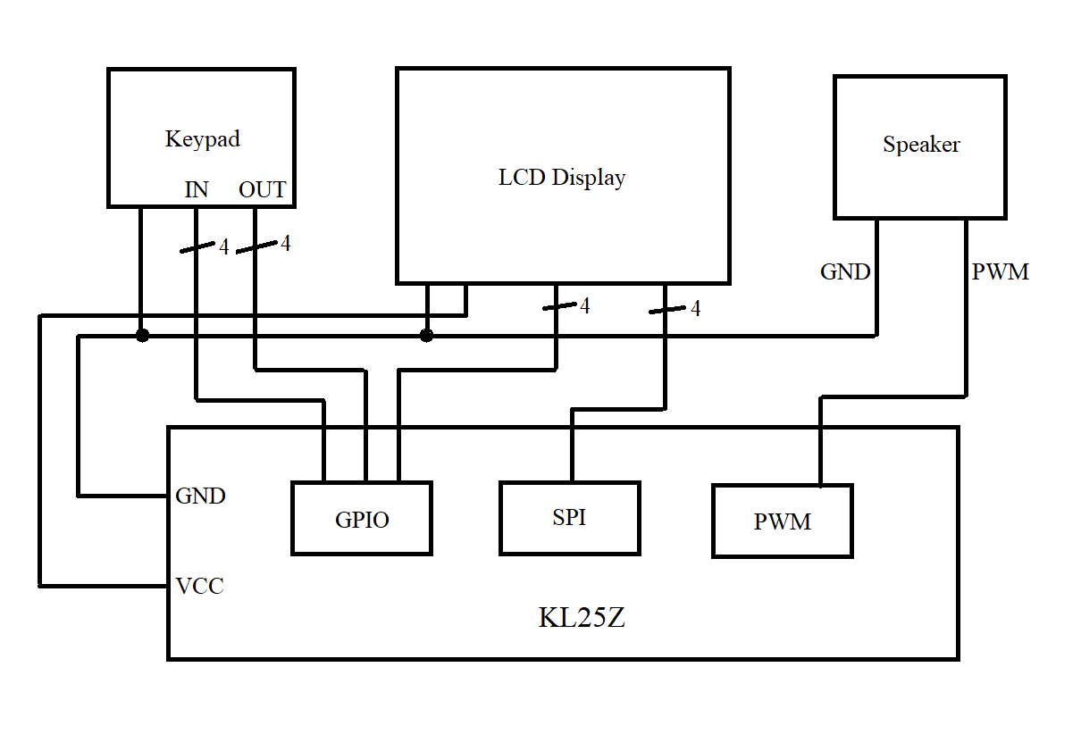
For our final project, we wanted to make 'handheld' console. On the software side, the FRDM-KL25Z acts as an emulator for the CHIP-8 instruction set and architecture. On the hardware side, we have a luxurious 160 by 128 pixel TFT LCD display, a 16 button multiplexed keypad with exposed wires and solder, and a piezoelectric buzzer speaker that brings back memories of deciphering motherboard error codes. Our firmware consists of a custom SPI driver to communicate with the ST7735R chip that drives the LCD (this part took up two full weeks of my life and required borrowing a $5000 oscilloscope, see #670), a GPIO pin multiplexer that reduces the number of required pins for the keypad from 16 down to 8 (plus ground), and a square-wave generator using the TPM/PWM module to generate a 440 Hz tone. The system can be powered from any 5 volt supply such as a dollar-store battery bank, your laptop's USB port, or lots of lemons.
/s
Background
CHIP-8 is an interpreted programming language used for simple computer systems such as the COSMAC VIP, DREAM 6800, and ETI 660 in the late 1970s. The output was generally displayed on a television, had at most 4K of RAM, and used 16 keys for input.
Software Overview
Memory Layout
The CHIP-8 can access up to 4KB of RAM. The first 512 bytes are reserved for the interpreter and contain other relevant data that can be used in a program, such as the font set.
The Memory Map, taken from the source listed at the end, is shown below.
+---------------+= 0xFFF (4095) End of CHIP-8 RAM
|               |
|               |
|               |
|               |
|               |
| 0x200 to 0xFFF|
|     CHIP-8    |
| Program / Data|
|     Space     |
|               |
|               |
|               |
|               |
|               |
|               |
+---------------+= 0x200 (512) Start of most CHIP-8 programs
| 0x000 to 0x1FF|
| Reserved for  |
|  interpreter  |
+---------------+= 0x000 (0) Start of CHIP-8 RAM
Registers
CHIP-8 utilizes 16 8-bit registers, which are indexed by a hexadecimal digit x. Each register is then referred to as Vx, and is used to store general data. Register VF is used to store flags.
An additional 16-bit register I is used to store memory addresses. CHIP-8 also contains two 8-bit registers reserved as timers for sound and delay. While these registers are not zero, they are decremented every clock tick (60 Hz).
CHIP-8 has a 16-bit program counter, denoted as PC, which stores the currently executing memory address. The language also uses an 8-bit register SP that points to the top of the stack.
The stack is an array of 16 16-bit values which is used to store the return address of a subroutine.
Keyboard
The keyboard is arranged as follows:
| 1 | 2 | 3 | C |
|---|---|---|---|
| 4 | 5 | 6 | D |
| 7 | 8 | 9 | E |
| A | 0 | B | F |
Display
CHIP-8 uses a 64x32-pixel monochrome display arranged as follows:
|
(0, 0) |
(63, 0) |
|---|---|
| (0, 31) | (63, 31) |
CHIP-8 draws graphics on the screen using sprites. Sprites are a group of bytes that form a binary representation of an image. The maximum possible sprite size is 8x15.
Font Set
The font set is a specific group of predefined sprites that represent the hexadecimal digits 0 through F. These sprites are all 5 bytes long and have dimensions 8x5. They are stored in the reserved area of memory between addresses 0x000 and 0x1FF.
For instance, the digit 3 is represented as:
11110000
00010000
11110000
00010000
11110000
Or, in hex:
0xF0
0x10
0xF0
0x10
0xF0
Timers & Sound
Recall that CHIP-8 provides an additional 2 registers for sound and delay timing purposes. Both registers are actively decrementing every clock cycle when they are nonzero. While the sound timer register is greater than 0, the CHIP-8 buzzer will sound.
The produced sound has only one pitch, and its frequency is determined by us (the interpreters).
Instructions
The original CHIP-8 language contains 36 unique instructions which are all 2 bytes long and stored little-endian. Our implementation of the instructions will be described in further detail in the technical section.
Peripheral Systems Overview
The TFT LCD is driven by the ST7735R, an IC that we can communicate with over SPI. We start by initializing a channel of the KL25Z's SPI (serial peripheral interface) module and configure it as a master, meaning it controls communication over the bus. This is necessary since all data will be sent from the KL25Z to the ST7735R. The IC has its own set of instructions, so we send this data via SPI to set up the driver in the appropriate modes which turn on the display and allow data to be written to the screen.
For our audio, we utilize the TPM module to generate a PWM (pulse width modulation) signal. This signal is a square wave with a 50% duty cycle (meaning it is high only half of the time), and a frequency of 440 Hz. What makes this module different than PIT is that it can act according to different counting modes such as up only, or up-down-up, and also directly control an output pin.
Instead of having 16 different input pins measuring each of the 16 buttons, our keypad uses multiplexing to reduce this to 8 pins: 4 inputs and 4 outputs. The buttons are arranged in an array such that each button corresponds to a pair of input and output pins. By constantly turning on and off each input pin at a time, and reading the result, we can determine which of the 16 buttons was pressed.
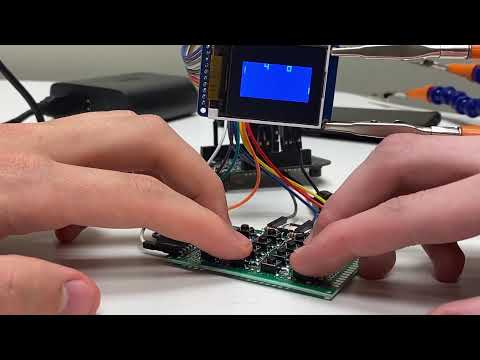
Project Video Demo
Click Thumbnail to Play
Technical Description
Structs
The CPU contains:
- An array of 16 8-bit registers used for representing each of the 16 Vx registers where x is a hexadecimal digit (0x0 to 0xF)
- A 16-bit I register generally used for storing memory addresses
- 8-bit delay and sound timer registers
- A 16-bit program counter pointing to the currently executing address
- An 8-bit stack pointer pointing to the top of the stack
- An array of 16 16-bit integers representing the stack
- A pointer to the bus for accessing other devices connected on the bus
- A 16-bit integer storing the value of the currently executing opcode
struct cpu {
	uint8_t  V[0xF]; // Vx registers where x is a hexadecimal digit
	uint16_t I; // I register
	uint8_t  DT; // delay timer
	uint8_t  ST; // sound timer
	uint16_t PC; // program counter
	uint8_t  SP; // stack pointer

	uint16_t stack[0xF]; // stack
	Bus_t*   bus; // pointer to the bus
	uint16_t opcode; // currently executing opcode
};
The CPU contains all of the registers, as well as the stack and a pointer to the bus. The pointer to the bus is later paired up with the bus struct, so the CPU can interface with the display and RAM.
The bus contains:
-
An instance of the CPU
-
An array of 8-bit integers the size of the Chip-8 display in pixels (2048-px) where each byte represents whether a specific pixel is turned on (1) or off (0).
-
An array of 8-bit integers representing the RAM of size 2048 bytes
struct bus {
	CPU_t    cpu;
	uint8_t  display[DISP_SZ];
	uint8_t  ram[RAM_SZ];
};
The bus is used as a virtual connection between the CPU and the display and RAM. Instructions are executed in the CPU, and their outputs are written to the display and RAM.
Functions
CPU
We use five functions that take in the CPU as a paramater:
void cpu_reset(CPU_t* cpu);
void cpu_timers(CPU_t* cpu);
void cpu_fetch(CPU_t* cpu);
void cpu_connect_bus(CPU_t* cpu, Bus_t* bus);
void cpu_execute(CPU_t* cpu);- cpu_reset resets all of the registers in the CPU to 0 and PC to 0x200 as this is the game's first instruction
- cpu_timers controls the delay and sound timers, decrementing them once every clock cycle
- cpu_fetch stores the next instruction in RAM into opcode using PC as an address
- cpu_connect_bus links the CPU's bus pointer to the bus struct so CPU can access the display/RAM
- cpu_execute decodes instructions and executes them
Bus
We also use several functions that take in the bus as a parameter to initialize the system.
void bus_init_display(Bus_t* bus);
void bus_clear_display(Bus_t* bus);
void bus_clear_ram(Bus_t* bus);
void bus_draw_border(Bus_t* bus);
void bus_load_font(Bus_t* bus);
void bus_load_game(Bus_t* bus, const uint8_t* game);
void bus_setup(Bus_t* bus);
void bus_write(Bus_t* bus, uint16_t addr, uint8_t data);
uint8_t bus_read(Bus_t* bus, uint16_t addr);- bus_init_display initializes the SPI and sets the screen's proper orientation.
- bus_clear_display fills the entire display with a blue rectangle
- bus_clear_ram sets every entry of the RAM array to 0
- bus_draw_border draws a border around the screen
- bus_load_font loads the numerical font into the reserved slots in the RAM
- bus_load_game loads the game instructions into the RAM starting at position 0x200
- bus_setup calls the above functions
- bus_write writes data to RAM[addr]
- bus_read returns data from RAM[addr]
We also use two functions to initialize the GPIO and PWM (for keyboard and sound respectively).
void bus_init_kb();
void bus_init_sound();- bus_init_kb initializes the GPIO for the keyboard
- bus_init_sound initializes the PWM for our speaker on the board
Finally, we use two simple functions to turn the sound on and off
void sound_on(void);void sound_off(void);Execution
Decoder
The decoder utilizes a few temporary variables for efficiency and legibility.
uint8_t x = ( cpu->opcode & 0x0F00 ) >> 8; //second most significant nibbleuint8_t y = ( cpu->opcode & 0x00F0 ) >> 4; //third most significant nibbleuint8_t n = cpu->opcode & 0x000F; //least significant nibbleuint8_t kk = cpu->opcode & 0x00FF; //least significant byteuint16_t nnn = cpu->opcode & 0x0FFF; //last three nibblesEach instruction is decoded into the above nibbles. Registers are also compartmentalized into the following variables, where x and y correspond to the above variables:
uint8_t* Vx = &(cpu->V[x]); //register Vx in cpuuint8_t* Vy = &(cpu->V[y]); //register Vy in cpuuint8_t* Vf = &(cpu->V[0xF]); //register VF in cpuDifferent instructions are identified by looking at the most significant nibble (MSN). Several switch statements break the opcode into around forty different instructions. Below is an example of the code required to decode and execute all the instructions with MSN=0,1,2.
switch( cpu->opcode & 0xF000 ) { case 0x0000: //switch on most significant nibble (MSN) switch( cpu->opcode & 0x000F ) { //two choices for MSN=0: 00E0 or 00EE so switch on least significant nibble (LSN) case 0x0000: //clear display bus_clear_display( cpu->bus ); break; case 0x000E: //return from subroutine cpu->PC = cpu->stack[cpu->SP--]; //set PC to its value before branching following calling convention (like a BL instr) break; default: break; } break; case 0x1000: //jump PC to address nnn in RAM, where nnn is last three nibbles of instr cpu->PC = nnn; break; case 0x2000: //call subroutine at nnn cpu->stack[++cpu->SP] = cpu->PC; //store current PC in stack, then branch cpu->PC = nnn; break;The outer switch statement discerns instructions by their MSN. The inner switch statement for MSN=0 discerns instructions by their least significant nibble, so the clear display instruction corresponds to 0x0??0 and the return from subroutine instruction corresponds to 0x0??E. From the manual, we identify these instructions to have opcodes 0x00E0 and 0x00EE respectively. Each of the roughly forty Chip8 instructions is decoded and then executed in this manner.
Main
The final component of the chip8.c file is the main method.
int chip8_main(void) { bus_setup( &bus ); bus_load_game( &bus, game ); cpu_reset( &(bus.cpu) ); cpu_connect_bus( &(bus.cpu), &bus ); while(1) { cpu_execute( &(bus.cpu) ); delay(10000); } return 0;}The bus_setup function is called first to initialize the display and RAM. Then, bus_load_game is called to load the game instructions into the RAM. Next, cpu_reset and cpu_connect_bus are called to initialize the CPU and pair it with the bus struct. Finally, cpu_execute is called to execute the next instruction in memory, and the delay function is called to emulate the 60Hz clock frequency of the Chip8. When the game is finished executing, the main method returns 0 to signify completion.
LCD Monitor
Hardware
The display is a TFT (think-film-transistor) LCD (liquid-crystal display) with a diagonal size of 1.8 inches and resolution of 128 by 160 pixels. CHIP-8 uses an 32 by 64 pixel display, so we chose to upscale that to 64 by 128 so each pixel is made up by 2 by 2 subpixels. While each pixel supports RGB, CHIP-8 only supports monochrome displays, so we have the choice of any two arbitrary colors for the 'sub-display', and any color for the border. The LCD is driven by the ST7735R, an LCD controller / driver IC (integrated circuit) that communicates over SPI (serial peripheral interface). The driver can receive data in an 8-bit or 9-bit mode. In the 9-bit mode, the first bit signifies if the incoming data is a 'command' or supplemental 'data'. In 8-bit mode, the IC uses an additional pin to determine the type of the incoming data.
Since the KL25Z SPI bus only supports sending 1-byte (8-bits) at a time, we opted to use the 8-bit mode and an additional GPIO bin for D/C (data/command). The SPI bus is also configured to use a clock polarity of zero (default low) and clock phase of zero (sample in middle of data) since that is the configuration that is recognized by the IC. The carrier board that connects the LCD and IC also has a CD74HC4050, a logic level shifter that makes sure that the incoming signals are converted to the appropriate voltage level and prevents damaging any components.
Pin Configuration
First, the clock to the zeroth channel of the SPI module is initialized by enabling its bit in SCGC4 (system clock gating register). Then, we initialize the clock to port C by enabling its bit in SCGC5. Port C was chosen since it includes pins that are mux-ed to the SPI module and has available GPIO pins. Each channel of the SPI module has two control registers (C1 and C2) which we used to set the clock phase (CPHA to 0) and clock polarity (CPOL to 0), configure as master (MSTR to 1), enabling slave select as an output (MODFEN to 1), enabling automatic control of slave select (SSOE to 1), disabling the SPI bus when not in use (SPISWAI to 1), and enabling the SPI bus (SPE to 1).
SPI0 also has two flags within the baud rate (BR) register for setting the baud rate / clock frequency of the SPI bus. In our case, we set the pre-scaler and scaler bits to zero such that the SPI frequency is the same as the peripheral bus frequency. Since we are using the 'default board files' configuration, the KL25Z core frequency is 48 MHz and the bus frequency is 24 MHz.
| Pin | Signal Name | Description | Mux Configuration | Notes |
|---|---|---|---|---|
| PTC0 | RESET | LCD & IC Reset | ALT1 (GPIO) | Active LOW |
| PTC3 | D/C | Select Data or Command Mode | ALT1 (GPIO) | Data LOW, Command HIGH |
| PTC4 | TFT_CS | Chip (Slave) Select for LCD | ALT2 (SPI0) | Active LOW |
| PTC5 | SCK | Serial Clock | ALT2 (SPI0) | Active HIGH |
| PTC6 | MOSI | Master Out Slave In | ALT2 (SPI0) | Active HIGH |
| PTC7 | MISO | Master In Slave Out | ALT2 (SPI0) | Unused |
| PTC10 | SD_CS | Chip (Slave) Select for SD Card | ALT1 (GPIO) | Always HIGH |
| PTC11 | LITE | Back Light Power | ALT1 (GPIO) | Always HIGH |
SPI Helper Functions
The SPI module can only send 1 byte at a time, so we started by implementing a Send_Byte function that takes a uint8_t, moves it into the data (D) register, and spinlocks until the buffer is empty by checking the transmission buffer empty flag (SPTEF), preventing us from overwriting unsent data. Next, we added Send_Data and Send_Command which take a uint8_t and appropriately control the D/C signal by setting or clearing PTC3 before sending the data.
LCD Helper Functions
Due to the complexity of the commands for initializing the LCD via the driver IC, we implemented the function Command_Helper. This processes an array of uint8_t formatted where the first number contains the number of commands to process, and each command contains an instruction, the number of data bytes, and the actual data. The details of the initialization are documented within externs.c and are based on Adafruit's Arduino library for the ST7735R.
The other helper functions implemented are: Set_Rotation, which tells the driver how to orient all future display commands; Command_Addr, a special function that manipulates the IC's screen buffer for pixel-by-pixel operations; Fill_Rect, which selects the location of the upper-left corner pixel and fills each pixel according to a width and length with a specific color; Fill_Screen, a modified version of Fill_Rect that just uses the position (0,0) and the screen's width and height; Draw_Pixel, which writes a color to a specific pixel given coordinates (x,y); and Clear_Screen, a modified version of Fill_Screen that uses the color black.
Speaker
According to the CHIP-8 specification, only a single tone is supported. To get a speaker working, we decided to use the TPM (Timer & PWM) module to generate a PWM (pulse-width modulation) signal at a certain frequency, and enabling its output when we want a sound. By nature, a PWM signal is a square wave which is good for our application of recreating a retro-console. First, the clock to the zeroth TPM module is initialized by enabling its bit in SCGC6. Then, we initialize the clock to port C by enabling its bit in SCGC5 since we will be using PTC9. This pin is set to alternative 3, which sets the mux to TPM0 (channel 5). Each TPM module can use a variety of clock sources, we want to select the 24 MHz signal generated from the PLL so we set PLLFLLSEL to 1 and TPMSRC to 1 within SOPT2 (systems options). Many different modes are available, but we will be using 'edge-aligned PWM'. To do this, we select the up-counting mode by setting CPWMS flag of the SC register.
To get a frequency of 440 Hz from the 24 MHz bus frequency, we need to select an appropriate pre-scaler and modulus value such that the frequency divided by the pre-scaler, divided again by the modulus is roughly equal to the requested value. Since the maximum pre-scaler value is 128 (2^7), we selected 426 for our modulus. To get a 50% duty cycle, the match value to modulus value needs to be in a 1:2 ratio, so we get the match value to 213. We then set both ELSA:B and MSB:A flags to 1:0 such that the PWM output goes high when it resets to zero (overflow past modulus) and goes low when it reaches the match value. For enabling the PWM output, we use the function PWM_On which enables the PWM counter by setting CMOD to 1 within the SC register. For disabling the PWM output, we use the function PWM_Off which disables the PWM counter by setting CMOD to 0.
Button Keypad
The specification requires a 16 button keypad, corresponding to each hexadecimal digit 0 to F. To avoid having to using 16 separate GPIO inputs for each button, we used a 4 by 4 array of buttons such that they can be multiplexed and reduce the number of GPIO pins required for the system to 8. Since the input pins sometimes float to the high state, pull-down resistors are added so the open state corresponds to ground. Below is a schematic of our keypad:
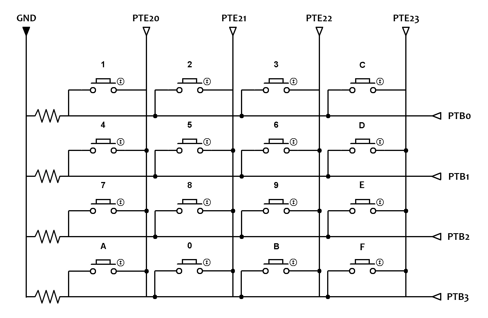
| Pin | Signal Name | Data Direction | Mux Configuration |
|---|---|---|---|
| PTB0 | IN0 | 0 (Input) | ALT1 (GPIO) |
| PTB1 | IN1 | 0 (Input) | ALT1 (GPIO) |
| PTB2 | IN2 | 0 (Input) | ALT1 (GPIO) |
| PTB3 | IN3 | 0 (Input) | ALT1 (GPIO) |
| PTE20 | OUT0 | 1 (Output) | ALT1 (GPIO) |
| PTE21 | OUT1 | 1 (Output) | ALT1 (GPIO) |
| PTE22 | OUT2 | 1 (Output) | ALT1 (GPIO) |
| PTE23 | OUT3 | 1 (Output) | ALT1 (GPIO) |
Since we are using both ports B and E, we need to enable both clocks to both using SCGC5. To enable the output of an individual pin, we implemented the function GPIO_On which takes a uint8_t which is a number 0 to 3. This is then added to 20 to get the the numbers 20 through 23. The equivalent bit of the PSOR register in PTE is set, enabling that pin's output. A similar process is done in the function GPIO_Off but setting a bit of PCOR, clearing the output. Lastly, the function GPIO_Read completes the entire multiplexing process to determine which button is pressed. First, one of the output lines is selected and enabled. We then initiate a read of the input port and mask off the last four bits corresponding to PTB0 to 3. We then disable the output, and if any input was high, we calculate the appropriate hexadecimal value corresponding to the pushed button. This occurs for all four outputs so all 16 buttons are checked during the four port reads. If no buttons are pressed, the value -1 is returned.
Testing
Due to the complexity of the project, it was necessary to test each part as its own module and also complete integration testing once the system was complete. To start, we needed to confirm the functionality of all 36 CHIP-8 instructions. We used a series of directed tests across every single instruction by calculating the functionality and state of the registers after the instruction, and comparing it to the actual result. This was mostly done to check edge cases. We also employed a random testing suite to confirm general functionality in the regular / trivial use cases. As we built the LCD driver, SPI was checked and debugged using the logic and bus analyzer present on the Tektronix MDO34. Each function was manually checked using visual inspection to confirm that the screen displayed the correct array of pixels with the appropriate colors. When we integrated the display into the CHIP-8 emulator, we were able to do compare the functionality with an web version of CHIP-8 using special test ROMs and certain games. As with other manual devices, the keypad needed to be tested directly by checking connectivity with a multimeter, and also using UART debugging once connected to the KL25Z. Since CHIP-8 only supports single buttons being pressed, the state of multiple buttons being pressed is left undefined. The speaker was able to be tested manually using an oscilloscope to inspect the PWM output, and listening to the output once connected. There are many automated test ROMs available online which we also used to triple-check instruction set functionality once all the peripherals were connected.
Credit & Attribution
No NXP fsl drivers were used in this project besides UART for debugging. While the SPI code is original, the ST7735R initialization arrays (Rcmd1, Rcmd2, and Rcmd3 in externs.c) and ST7735R helper functions are based on the Adafruit ST7735 Library for Arduino and are not completely original work.
The game ROMs used for testing and in the video presentation were created and/or found by user mir3z on GitHub.
The name Napptendo DS is parody has no affiliation with any similarly named companies and/or products. This project is not a commercial product, please do not sue us.
Resources & References
CHIP-8 Technical Reference Manual
1.8" Color TFT LCD display with MicroSD Card Breakout - ST7735R
ST7735R LCD Controller Datasheet
KL25 Sub-Family Reference Manual
Adafruit ST7735 Library for Arduino
Work Distribution
We did not encounter any issues with collaboration or work distribution. All tasks were split according to the description below, with the website and project video being completed together. All partners agree that the workload was split appropriately and each partner contributed equally to the project.
Arun Raman
- Memory and frame buffer emulation
- CPU register support
- Instruction set support
- Display driver integration
Harris Miller
- Custom bare-metal SPI driver
- TPM/PWM speaker driver
- GPIO keypad multiplexing driver
- Soldered protoboard keypad
- Driver integration testing
Raleigh Clemens
- Font set support
- Instruction set testing
- Keypad driver integration
- Speaker driver integration
Images & Appendix
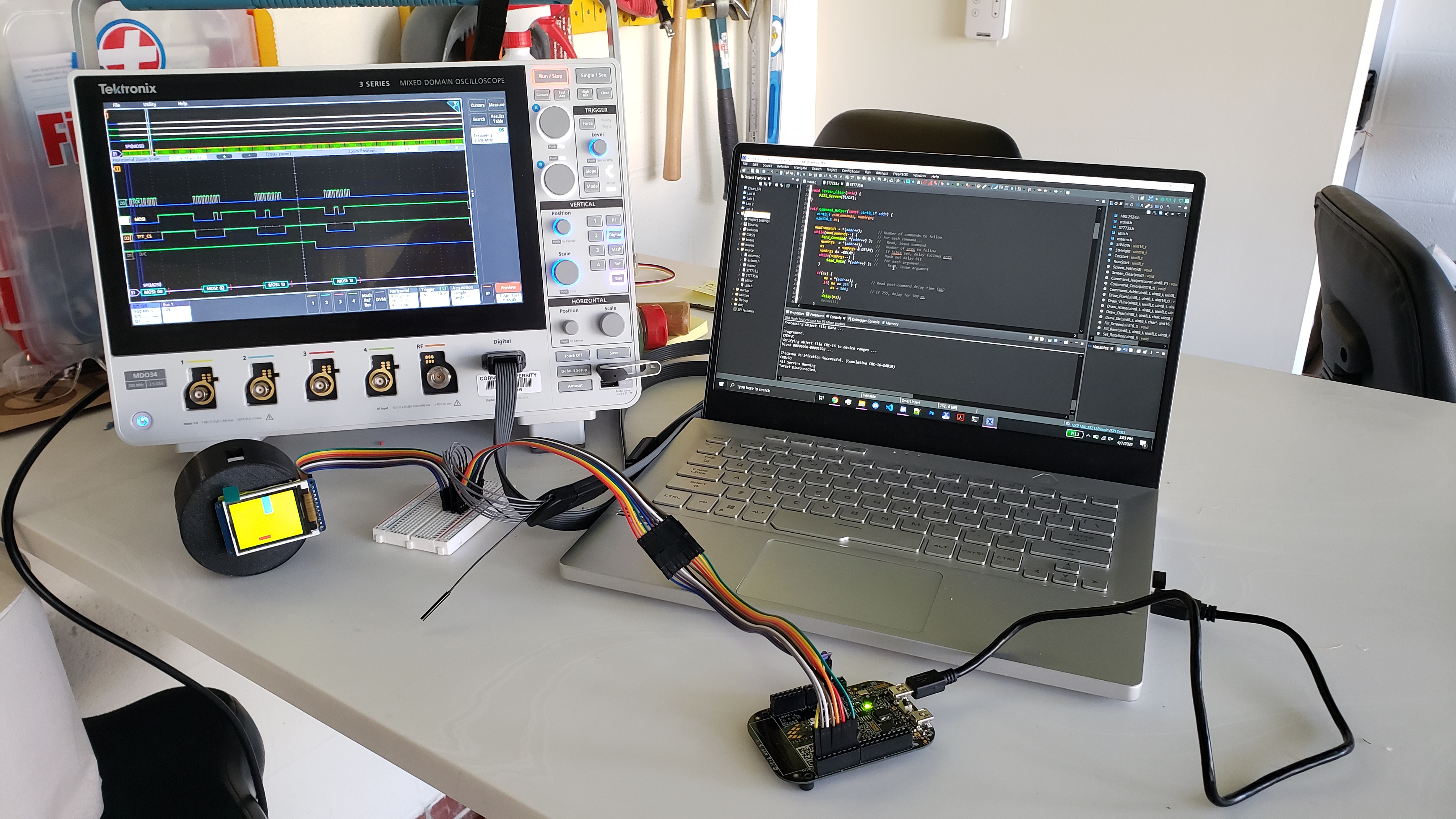
SPI debugging setup using a Tektronix MDO34, courtesy of Parker Miller and the Cornell Maker Club.
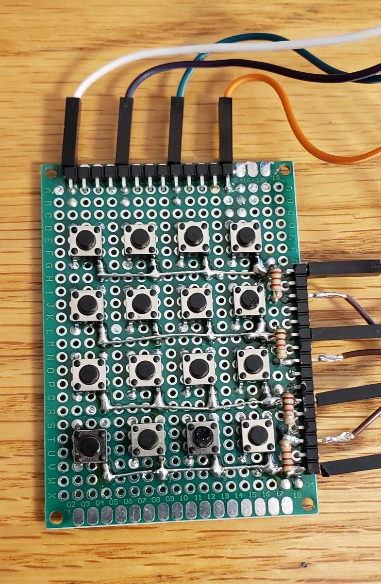
Our prototype 16 button keypad.
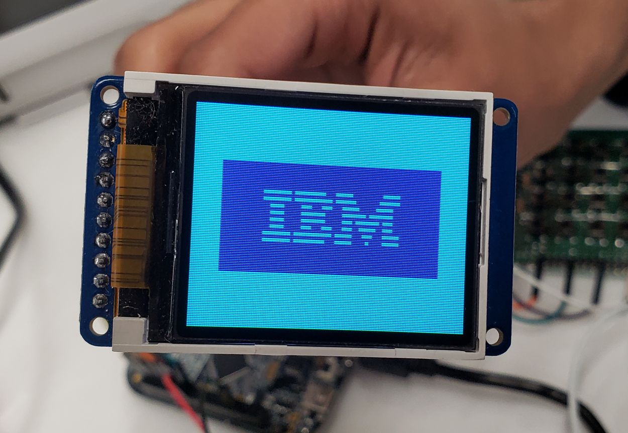
Picture of the IBM test program running on the KL25Z.
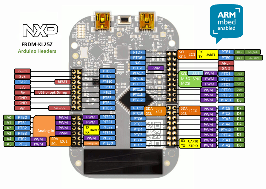
KL25Z Pins Diagram (technically incomplete due to lack of SPI0 on Port C).