Go To:
Home Page
PCB Tutorial
Introduction
This tutorial will discuss general considerations in PCB design and then narrow in on specific advice tailored to the constraints of ECE 3400. Information about what a PCB is can be found here; we will cover the essentials for designing the PCB.
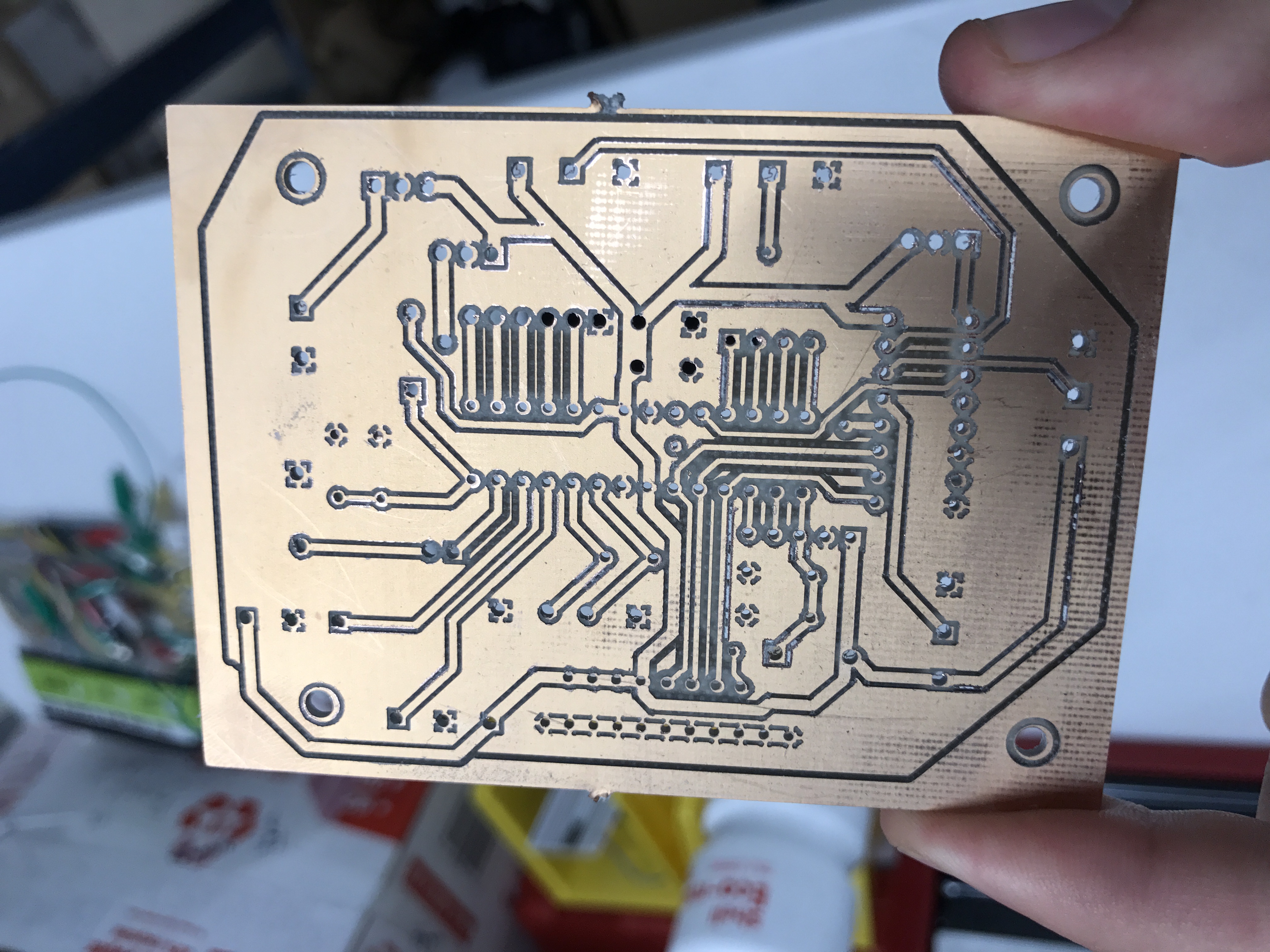
A PCB is extremely useful because you can route a lot of wiring in a compact and permanent manner. This can greatly reduce the headaches caused by misconnections and confusing wire paths. The idea is to replace all of the messy external wiring with connections on a PCB; these connections are are thin copper regions called traces and can be thought of as small wires. If you want to connect to the board externally, you can leave holes in these traces, or vias, for components to slide into.
Note: Surface mount components do not require a via, but are beyond the scope of this class
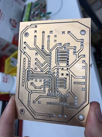
Here is an example of a board with traces between vias:
Design
The PCB design process begins with a schematic. Below is the schematic for our final PCB design: 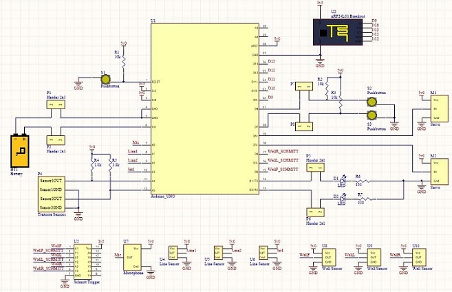
Note that every component is clearly labelled and its connections are as well. Wires can be drawn to connect pins, or you can name wires the same thing to signify that they are connected. The schematic must be clear so that other team members can inspect and verify the design. If the design is too complicated to show everything cleanly on one schematic, it should be separated into various schematics with various purposes. Here is an example of that with our first PCB design: PCBv0_Schematic
Note that the pins on the Arduino in the schematic do not correspond to actual pin numbers but rather pad locations for the layout
Once the schematic is complete, you should have at least one other person check the design before moving into layout. Layout is the fun part! Now we get to place all of the components and decide how they will connect. There are many considerations for layout but for a simple design here are some rules of thumb:
- Make high-current traces thicker and short if possible
- Make high-frequency traces (like serial communication) short and without many turns
- Make ground a large plane so that you don’t need a wire for every component to connect to it
- Add capacitors between GND and VDD to decouple voltage spikes
- Power servos separate from sensitive analog circuitry for the same reason
- Mind your tolerances
Note: Tolerances are the limits of your PCB manufacturer (like space between edge of board and components, thickness of traces, minimum width between traces, etc). We milled the PCB ourself so these were larger than normal
We want to minimize the trace lengths ideally, but we also need to put all of the components in sensible locations for the robot. This may take some practice and iteration, but is very important so that the final design is useful. In our case, we were using the PCB mill which requires hand-inserted vias. To avoid this annoyance, I placed components so that they could almost all be routed on the bottom (blue) layer. The few traces which did intersect were routed to vias so that they could be connected with wire.
Here is the layout for the final schematic shown above: 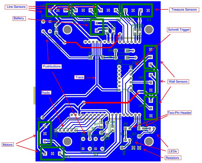
Note: The entire bottom layer is a ground pour
Manufacturing
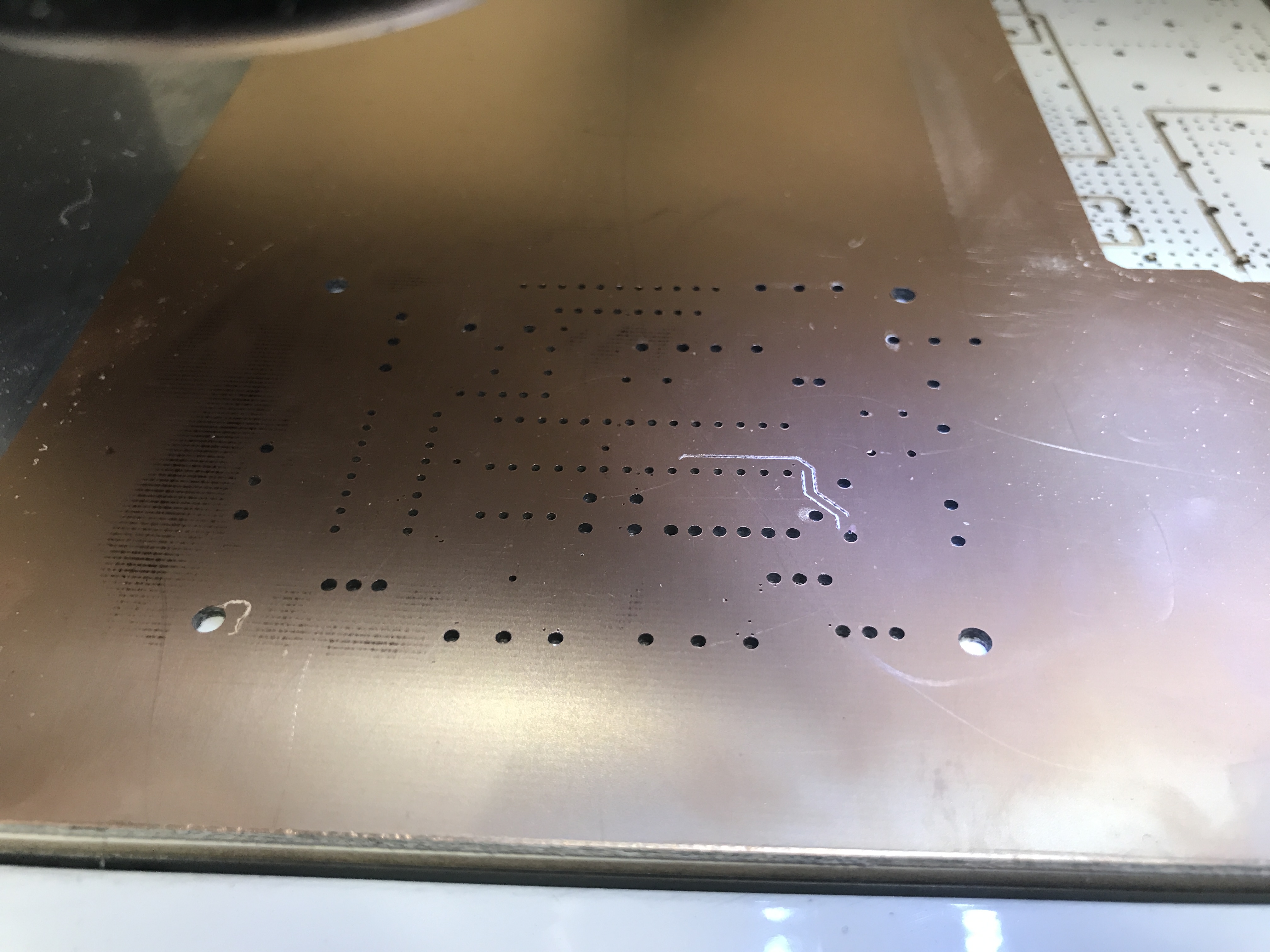
Now we are ready to mill the board. This part is not essential, but illuminates one method of creating a PCB. It consists of cutting away the copper between traces and around drill holes so that various parts of the boards are not shorted together. First, we run the drill layer and end up with the following result:
Then we run the top and bottom layers which cut away copper until we have traces between the drill holes and leaving something which lookes like the following image. The black lines are places where the copper has been cut away, creating thin copper traces between.
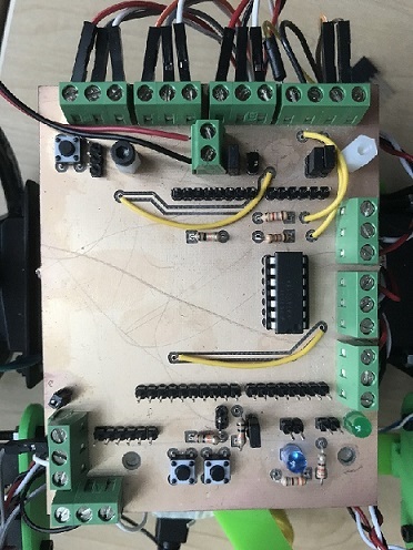
Next, we need to populate the board. This consists of gathering all the components and soldering them on, verifying their location using the schematic and layout pictured earlier. After populating the board, it looked like this:
Testing
After soldering everything on,
it is extremely important to follow a strict testing procedure before connecting any electronics and potentially damaging them or yourself.
Using a multimeter you should:
- Visually inspect all solder and check that nothing crosses over isolations
- Check continuity between the component and the trace it is soldered to (Should be <1ohm)
- Check continuity between the trace and adjacent ones (Should be infinite resistance)
- If the bottom is a ground plane (which it was in our case) then check the resistance between the soldered component and ground (Should be infinite unless they are connected via resistor)
Note: When turned off, a voltage regulator will actually create a non-infinite resistance between ground and the 5V trace. (about 13k in our case)*
After verifying all of the traces in the above process, you are still not ready to attach electronics. Now you should do the initial power-on test. Wire up a battery or DC voltage source to the input terminals on the board and verify that all power rails are at the proper voltage and the input current is reasonable for what is connected.
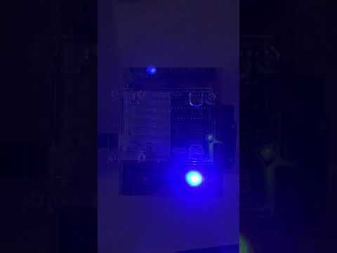
Finally, you can attach all of the electronics and continue the testing procedure. In our case, this consisted of checking the input and output of every pin on the Arduino, ensuring that it was connected to everything properly. The first test we did was run Blink() with attached LEDs:
Advice Tailored to 3400
1) Modularity
A PCB is great because it provides a reliable, permanent connection. This can be a big downside, though, when you realize some part of the design needs to be modified. Whereas you could quickly swap something on breadboard, PCBs are much harder to alter. While extensive design verification is great, it won’t cover every problem which may arise. We prioritized modularity in our design by connecting many Arduino pins through two-pin headers, allowing us to connect and disconnect the pushbuttons, battery, and LEDs at will using the small header short pictured below. This offers the robustness of a PCB, while still being modular like a breadboard. We highly recommend using these for simple PCB designs: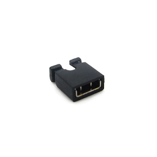
2) Print and Check Everything
We ran into issues with the wire coming from the serial port hitting the wheel, so we couldn’t run our robot while the computer was plugged in to the computer (we circumvented this issue using header extenders). This could have greatly inhibited iteration and ruined the design. I strongly recommend printing the layout and checking that all components will fit properly.
3) Consider Ease of Use
Initially, we wanted to remove the Arduino and just use the AVR microcontroller itself. Basically a PCB version of our Boarduino:
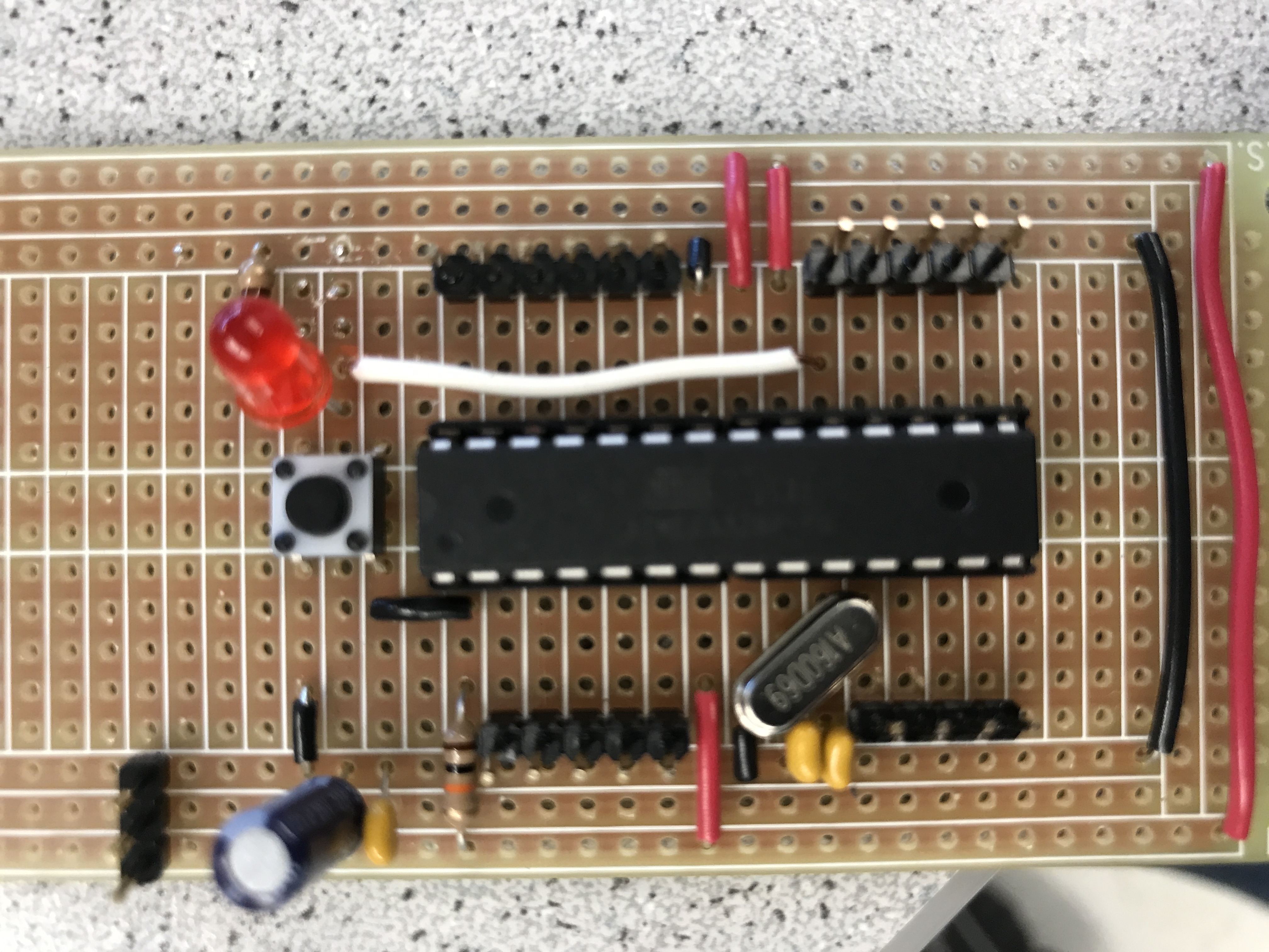
This was a poor idea, though, because we could not program via serial and needed to hook up a few wires to program it each time. It is extremely important to have the ability to iterate quickly and debug thoroughly in this class, so we ended up overhauling the design completely and using the Arduino Shield design shown above.
We were able to successfully incorporate the PCB onto our robot and it worked great. We recommend designing and utilizing one for the learning experience as much as the benefit toward robot robustness. Good luck!
Go To:
Home Page