Objective
Our goal was for the arduino to communicate with the base station FPGA and draw something on the monitor. In our case, we chose to draw a square whose color continously changed depending on the arduino output to show that our arduino/FPGA connection is working correctly.
Materials
- 1 20 kOhm Resistor
- 1 30 KOhm Resistor
- 1 DEO Nano FPGA
- 1 VGA Adapter
- 1 Breadboard
- Arduino Uno
- DAC circuit board
- Solder and Soldering Iron
- VGA cable
- VGA connector
Arduino to FPGA Hardware
We use parallel protocol for sending data from the arduino to the fpga. Originally, we were going to use SPI, but we found parallel to be faster and simpler to implement. since the base station's arduino will only be connected to the display, we did not need to worry about saving digital pins for other tasks. So, using a parallel connection was ideal for this case.
For this lab, our Arduino sent alternating high and low values (with a half second delay) to one of our fpga's gpio pins.
As seen below, the output from the digital pin 13 on the Arduino is passed through a voltage divider and then into the GPIO 1 pin 20 which corresponds to GPIO_1_D[15] on our FPGA. As we progress towards milestone 4, we will incorpoarte more gpio pins on the arduino and fpga to correctly draw our maze. We will have 12 arduino signals parallely connected to the FPGA. There will be 4 pins each for the X and Y coordinates, 3 pins for the obstacles on the left, right and in front of the robot and possibly 1 pin to indicate the direction (N, S, E, W).
The diagram below shows connections between the arduino to FPGA and FPGA to the monitor.
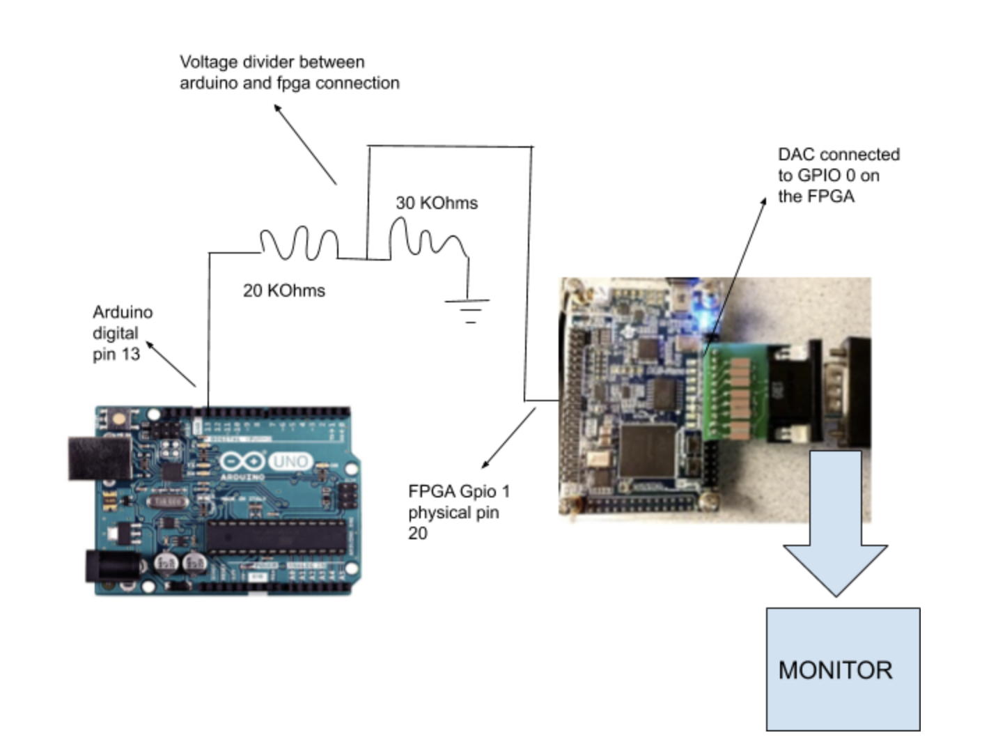 Hardware layout
Explanation of Voltage Divider
As seen above, we use a voltage divider between the arduino and the FPGA to convert a 5V output from the Arudino to an ~3V input to the FPGA. The FPGA runs on 3.3 V. Due to inconsistency in actual resistor values, we aimed to send a signal to 3V to the FPGA to prevent our signal from crossing the 3.3V threshold. To calculate resistor values, we used the equation Vout = Vin * R2/(R1 + R2) with R2 being the resistor that is grounded. To get 3V as Vout, we needed to multiple a ratio of 3/5 to our 5V Vin. So, we chose R1 to be 20KOhms and R2 to 30KOhms. This helped us achieve the desired ratio and this is how we created a voltage divider for our FPGA input.
Creating a functional DAC
The FPGA outputs a digital signal to represent color, with three bits for red, three bits for green, and two bits for blue. However, the VGA connector only takes in analog inputs for color. To fix this issue, we used a breakout PCB board connecting the FPGA to the VGA, with differing resistor values to change the three or two bit signals into an analog value between 0 and 1V. The connector itself was given to us by the TAs, with values that reflected the values Bruce Land used on his Hackaday page. These values assign different weights to each pin's voltage, so that it scales with a more significant bit contributing to a higher voltage on the DAC output.
Arduino Code for parallel communication
	    // Toggling pin 13 high and low
            void loop() {
              digitalWrite(13, HIGH);
              delay(500);
              digitalWrite(13, LOW);
              delay(500);
            }
FPGA Code
With the high and low values from the arduino, we alternated the color of the square that was being drawn on the monitor. A high value from arduino corresponded to a yellow square, and low value was red.
Below is our always block for our image processor module. This is how we are able to draw the square. We increment the address such that we iterate through one row at a time in a 30x30 square. Each time the array address updates, the color of that address is set based on the value from the Arduino "GPIO" input. In future, we will update this code to take in more complex data from an arduino and map a maze.
always@(posedge CLK) begin
	if (X_ADDR < 18'd30) begin //continue along row, increment column
		X_ADDR = (X_ADDR + 1);
		Y_ADDR = Y_ADDR;
		W_EN = 1'b1;
	end
	else if (X_ADDR == 18'd30 && Y_ADDR < 18'd30) begin //go to next row, reset column
		Y_ADDR = (Y_ADDR + 1);
		X_ADDR = 18'd0;
		W_EN = 1'b1;
	end
	else begin //finished 30x30 square, reset addresses and repeat
		X_ADDR = 18'd0;
		Y_ADDR = 18'd0;
		W_EN = 1'b0;
	end

	//Set color based on gpio input
	if(GPIO == 1'b1) begin
		color = 4'b0001; //yellow
	end
	else begin
		color = 4'b1111; //red
	end


	//set color
	if (W_EN == 1'b1) begin //set result to color determined by arduino
		RESULT = color;
	end
	else begin
		RESULT = 4'b0000; //green
	end
end
This diagram represents the signals and instantiated modules in our DEO_nano.v file. You can see here how the information about address and color, which come from the image processor module, are sent to other modules. The x_addr and y_addr are used for the write address which is calculated in the deo_nano file. The color is stored in the "write address" location in memory (M9K RAM) during the positive clock edge of clk_W which operates at 50 MHz if the write enable to memory is high. When we want to stop storing data in memory, we set the write enable to low. At the positive clock edge of clk_R which operates at 25 Mhz (since we want reading to be slower than writing so that updated information is always read), the information stored in memory is written to the output from the M9K ram module. This output is then used to determine the input to the VGA driver module which is then displayed on the monitor. The diagram below shows how information flows through the different components of our code.
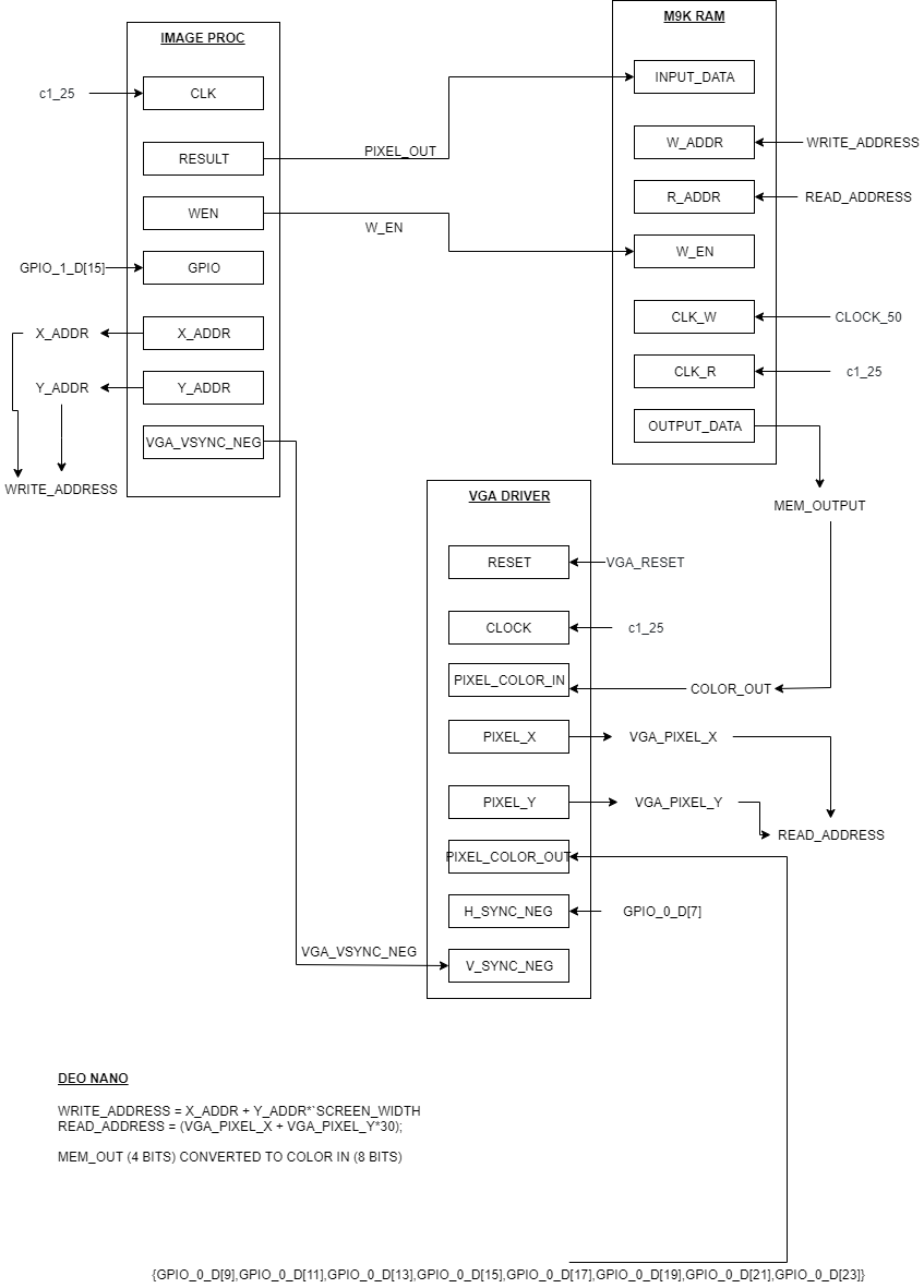 Diagram showing the signals and instantiated modules in our DEO_nano.v file
The video below shows the final output on the monitor.
FPGA updates color based on signal from ArduinoTherefore, we were successfully able to send signals from our base station's arduino to our FPGA and make the drawing on the monitor change color based on the arduino input.