Lab 3
Objective:
The purpose of this lab was to create a video controller with an FPGA, controlled by an Arduino Uno. To do this, we familiarized ourselves with the DE0-Nano FPGA development board, developed a system for transferring image information from the Arduino to the FPGA, and learned how to interact with the video memory and VGA driver.
Materials:
- DE0-Nano Development Board
- Arduino Uno
- Various resistors
- Empty DAC circuit board
- Solder and Soldering Iron
- VGA cable
- Female header
- VGA connector
Communication Method:
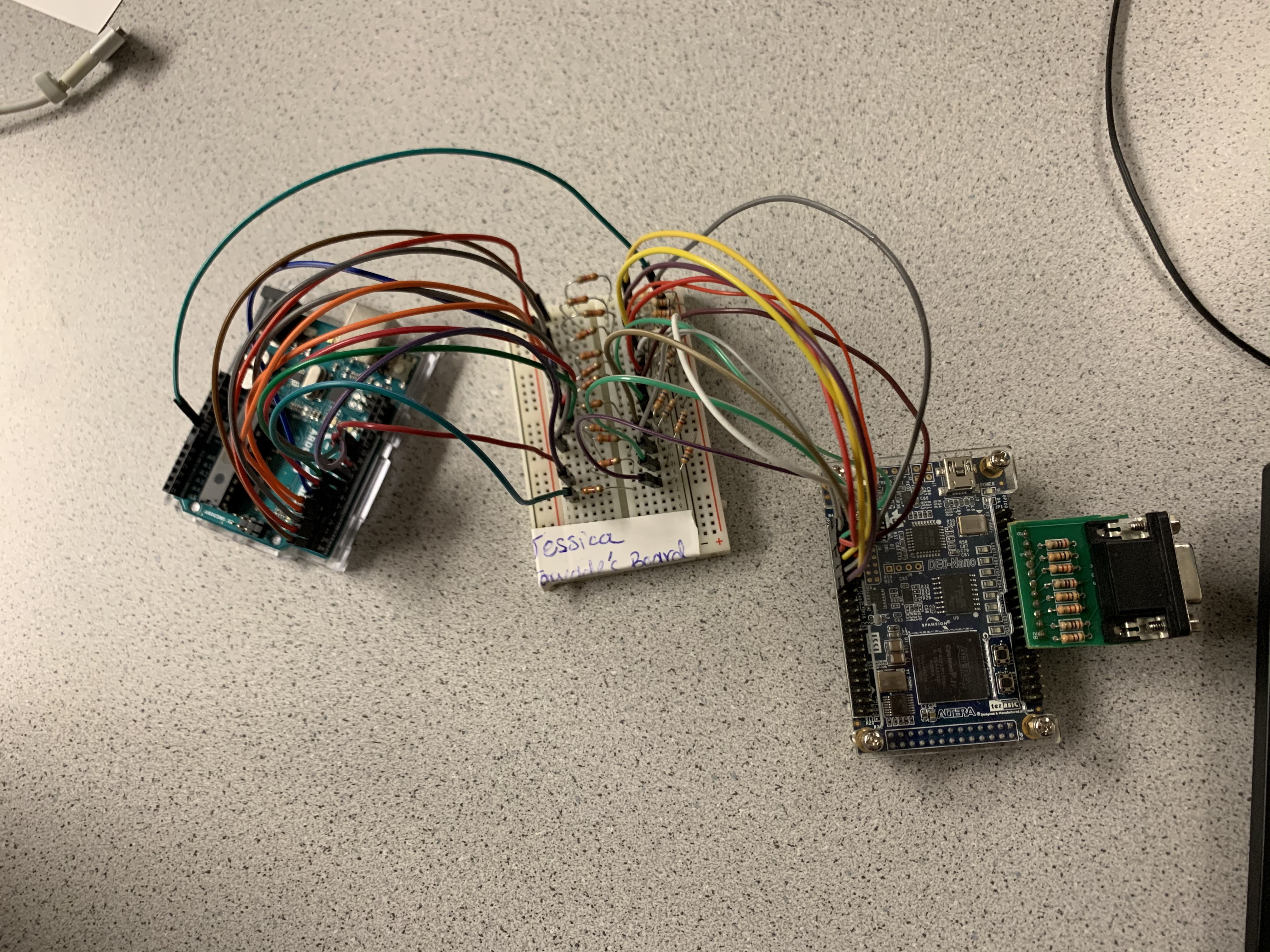
For our Arduino-to-FPGA communication protocol, we chose to implement a parallel interface using 12 GPIO pins - one for each bit. The parallel setup can be seen in Figure 1 below. Looking ahead to the robot competition, where we must navigate a 9x9 grid, we have 4 bits to signify an x-coordinate, 4 for a y-coordinate, and a bit to signal a wall for each of the four cardinal directions. The way these relate to the display will be explained in the next section.
We chose to implement a parallel communication protocol after we were unable to get an SPI interface working properly soon enough. The Verilog and Arduino implementation for parallel came to us more easily, and we do not foresee issues changing it to fit our evolving needs going forward.
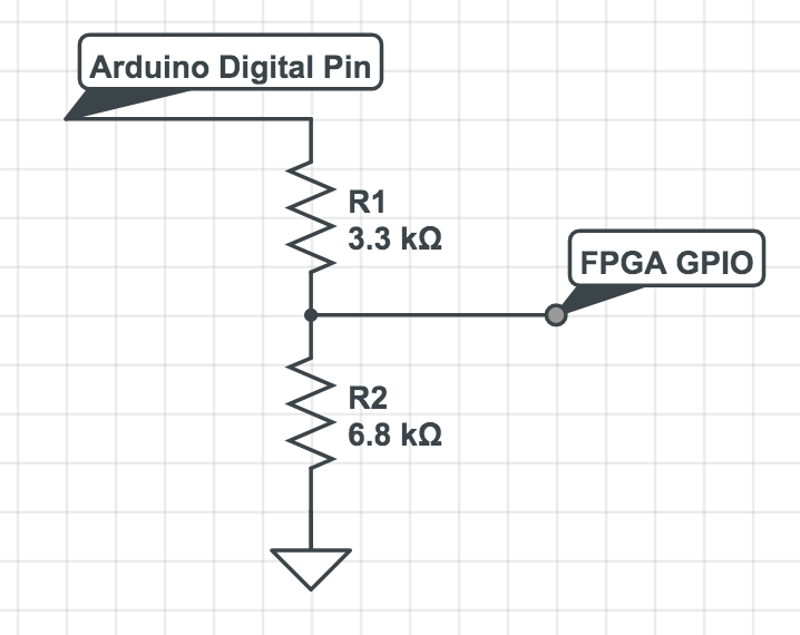
The physical circuit used to implement this is quite simple. Each of the 12 arduino pins has a voltage divider between it and the FPGA pins. The Arduino outputs 5 volts on its digital pins while the DE0-Nano uses 3.3V. As a result, the voltage dividers made sure that the input voltage to the FPGA pins were within the operating range. Since the FPGA pins are the ones receiving an input, we have tied them to pull-down resistors. Figure 2 shows the schematic of the voltage dividers in relation to the Arduino and FPGA.

Figure 1: Parallel Communication Protocol Between Arduino and FPGA

Figure 2: Arduino-FPGA Voltage Divider
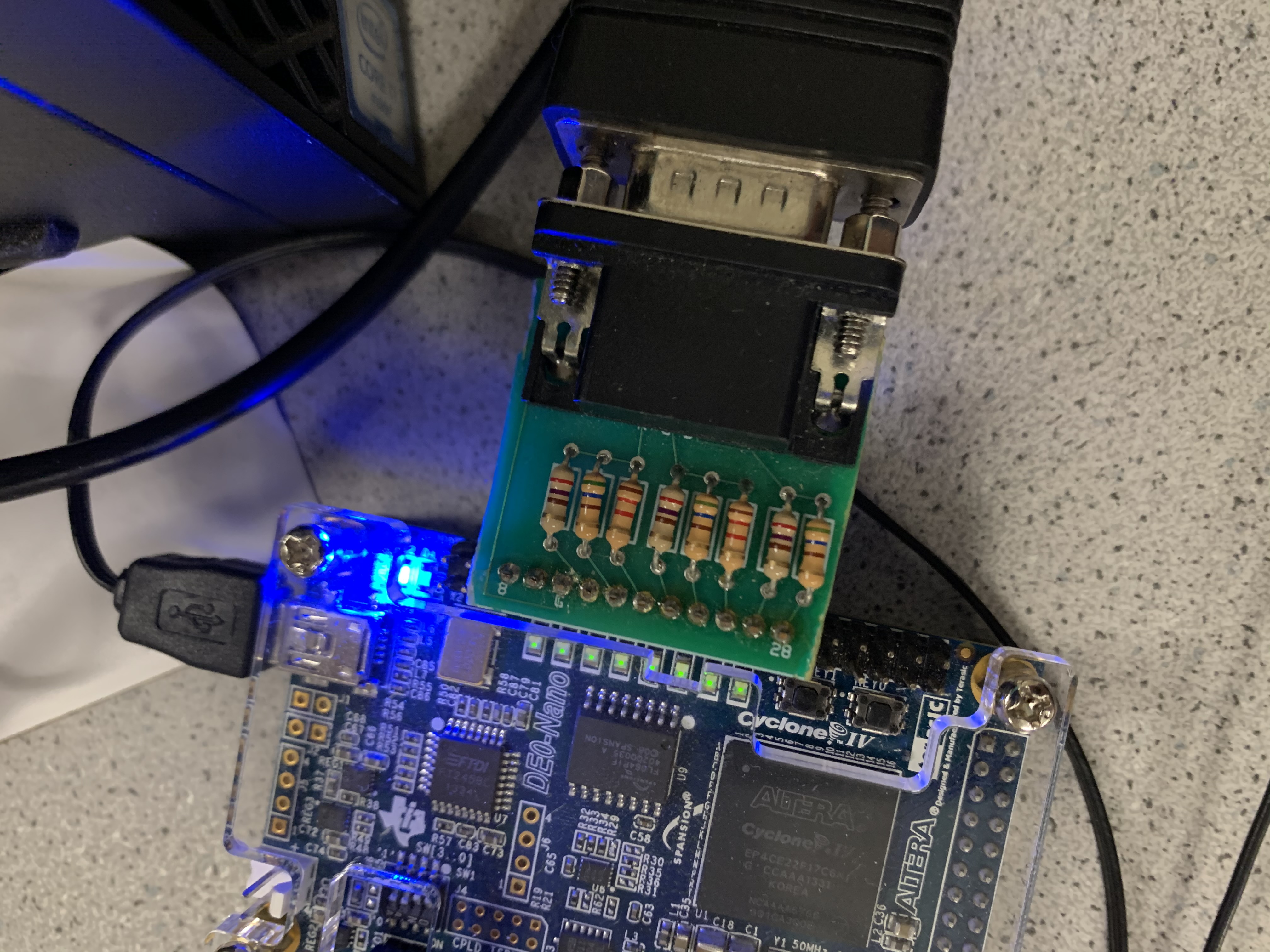
As for the FPGA-to-monitor communication, the FPGA relays information to the screen via VGA cable. There is a DAC between the FPGA and the VGA cable so that the cable gives analog values in RGB format to the screen. The DAC uses resistors to convert each bit in a 3-bit digital signal to analog by dividing the most, middle, and the least significant bit of each color signal by different values and combining the analog outputs of each bit together to get a different voltage level for every different digital value. The DAC was provided to us by the TAs with the resistor values calculated by Professor Bruce Land. The design of the DAC can be seen in Figure 3 below.

Figure 3: Design of the DAC
Drawing on the Display:
Given the input to the FPGA as described above and our looking ahead to the competition, we chose to draw on the screen by dividing it into a 9x9 grid and drawing coloring edges of each of these blocks based on arduino input. The x- and y- coordinate bits tell which block to color if needed, and the other four bits for the walls determine which edges of the block must be colored. Our vision for the robot competition is to have a system like this where the coordinate bits are the location of the robot, and the edges of the box represent possible locations of a wall.
Since our usable pixels on the screen are directly mapped to the M9K memory module, we must calculate the addresses to update in memory so that an edge is properly displayed. We first calculate which “block” on the grid we are in by doing some arithmetic on the coordinates given from the arduino. From there, we write red to the corresponding memory addresses if any of the wall bits are high.
For example: the memory address of the top left corner of a block (x, y) is: (270*30*y) + (30*x)
From there it is not too difficult to come up with how to write only an outer edge using offsets. We added some additional logic that ensures that the Write Enable signal to the M9K is only high when it needs to be writing to a wall, and it always writes red.
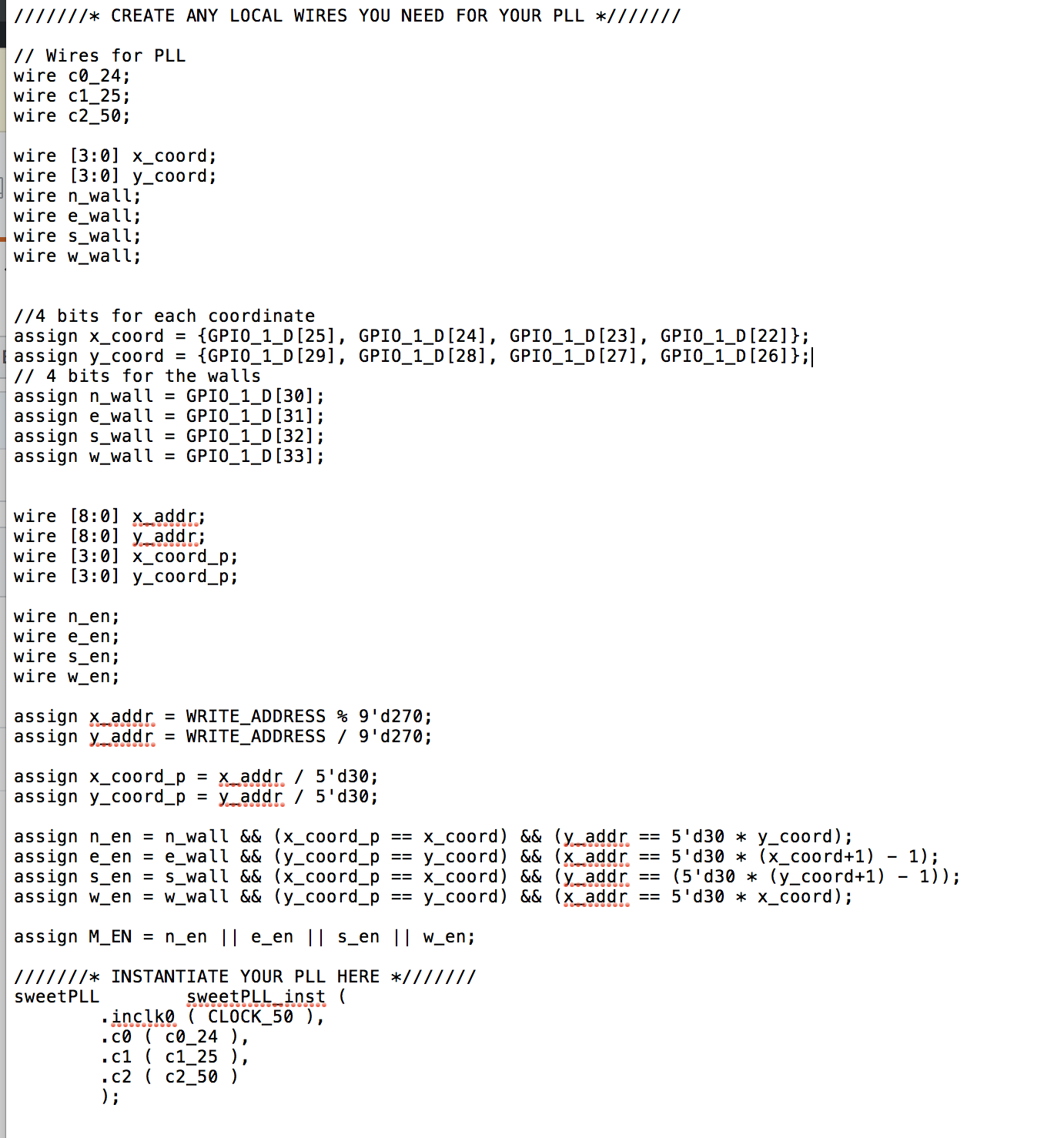
The VGA driver module then cycles through the range of pixels on the display, outputting the value in memory at the corresponding address to that pixel if the pixel is within the 270x270 square in the top left corner of the screen, or the color blue if the pixel is outside that range. The memory can be read from and written to at the same time, so the Arduino can interface with the FPGA in parallel with the VGA display. The input from the Arduino determines the read address to the M9K (using similar math to the example shown above) and the write address is that for the pixel referred to by the VGA driver. The logic described above can be seen in the verilog Code Snippet 1 below.

Code Snippet 1: VGA Display Verilog Code
Displaying the Smiley Face Design:
We wrote a simple arduino program that displays a smiley face to the monitor! Pins 0-3 represent the x-coordinate, pins 4-7 represent the y-coordinate, and pins 8-11 represent the walls (8 for north, 9 for east, etc.). Using a helper function that simply writes all the pins to any desired pattern, we wrote a smiley face block by block. One full square for each eye and the nose, and 6 square fragments to make up the mouth. The arduino outputs a sequence, delays, outputs the next sequence, delays, and so on. The code described above can be seen in Code Snippet 2 below and the result can seen in Video 1 below.
// 4 pins (bits) for x coordinate
int x0 = 0;
int x1 = 1;
int x2 = 2;
int x3 = 3;
// 4 pins (bits) for y coordinate
int y0 = 4;
int y1 = 5;
int y2 = 6;
int y3 = 7;
// 4 pins for walls
int Nwall = 8;
int Ewall = 9;
int Swall = 10;
int Wwall = 11;

void setup() {
  // Set all pins as outputs
  pinMode(x0, OUTPUT);
  pinMode(x1, OUTPUT);
  pinMode(x2, OUTPUT);
  pinMode(x3, OUTPUT);
  pinMode(y0, OUTPUT);
  pinMode(y1, OUTPUT);
  pinMode(y2, OUTPUT);
  pinMode(y3, OUTPUT);
  pinMode(Nwall, OUTPUT);
  pinMode(Ewall, OUTPUT);
  pinMode(Swall, OUTPUT);
  pinMode(Wwall, OUTPUT);
  // Initialize all pins
  writeAPlace(0,0,0,0,0,0,0,0,0,0,0,0);
  delay(5000);

  // Draw each component of the smiley face
  // All 4 Walls on (3, 2)
  writeAPlace(0, 0, 1, 1, 0, 0, 1, 0, 1, 1, 1, 1);
  delay(500);
  // All 4 walls on (5, 2)
  writeAPlace(0, 1, 0, 1, 0, 0, 1, 0, 1, 1, 1, 1);
  delay(500);
  // All 4 on (4, 4)
  writeAPlace(0, 1, 0, 0, 0, 1, 0, 0, 1, 1, 1, 1);
  delay(500);
  // NEW on (2, 5)
  writeAPlace(0, 0, 1, 0, 0, 1, 0, 1, 1, 1, 0, 1);
  delay(500);
  // NEW (6, 5)
  writeAPlace(0, 1, 1, 0, 0, 1, 0, 1, 1, 1, 0, 1);
  delay(500);
  // WS on (2, 6)
  writeAPlace(0, 0, 1, 0, 0, 1, 1, 0, 0, 0, 1, 1);
  delay(500);
  // ES on (6, 6)
  writeAPlace(0, 1, 1, 0, 0, 1, 1, 0, 0, 1, 1, 0);
  delay(500);
  // NS on (3-5, 6)
  writeAPlace(0, 0, 1, 1, 0, 1, 1, 0, 1, 0, 1, 0);
  delay(500);
  writeAPlace(0, 1, 0, 0, 0, 1, 1, 0, 1, 0, 1, 0);
  delay(500);
  writeAPlace(0, 1, 0, 1, 0, 1, 1, 0, 1, 0, 1, 0);
  delay(500);
}


void loop() {
  delay(1000);
}
// Writes the values of all the pins
void writeAPlace(int X3, int X2, int X1,int X0, int Y3, int Y2, int Y1, int Y0, int N, int E, int S, int W){
  if (X3) digitalWrite(x3, HIGH);
  else digitalWrite (x3, LOW);
  if (X2) digitalWrite(x2, HIGH);
  else digitalWrite (x2, LOW);
  if (X1) digitalWrite(x1, HIGH);
  else digitalWrite (x1, LOW);
  if (X0) digitalWrite(x0, HIGH);
  else digitalWrite (x0, LOW);
  if (Y3) digitalWrite(y3, HIGH);
  else digitalWrite (y3, LOW);
  if (Y2) digitalWrite(y2, HIGH);
  else digitalWrite (y2, LOW);
  if (Y1) digitalWrite(y1, HIGH);
  else digitalWrite (y1, LOW);
  if (Y0) digitalWrite(y0, HIGH);
  else digitalWrite (y0, LOW);
  if (N) digitalWrite(Nwall, HIGH);
  else digitalWrite (Nwall, LOW);
  if (E) digitalWrite(Ewall, HIGH);
  else digitalWrite (Ewall, LOW);
  if (S) digitalWrite(Swall, HIGH);
  else digitalWrite (Swall, LOW);
  if (W) digitalWrite(Wwall, HIGH);
  else digitalWrite (Wwall, LOW);
}
Code Snippet 2: Smiley Design to the Monitor
Video 1: Displaying a Design to the Monitor
Looking Ahead:
We realize that using 12 digital pins for serial communication could be too much once we must connect the radio to the base station, so this is likely not the exact method we will be using for the competition. It worked for the purpose of this lab and we began to think about how to best represent the data needed during the competition, but we are ready to cut down the amount of bits in the parallel communication if we must.