Lab 3: Using An FPGA
For Lab 3 we divided into two subteams: Graphics and Acoustic
Graphics Team:
- Logan
- Trisha
- Francis
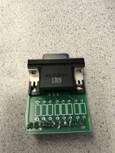
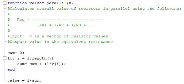
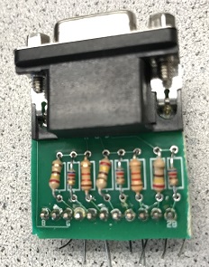
In order to connect to the computer via VGA cable, we first needed to wire the Digital-to-Analog Converter (DAC) for the connector. The FPGA outputs digital signals at 3.3V, while the computer reads analog values of voltage from 0-1V through the VGA port. That means we need to add a resistor DAC for the conversion. The VGA connector without resistors is shown below.
The data is structured in the following way:
- 3 bits for red (Bits 7-5)
- 3 bits for green (Bits 4-2)
- 2 bits for blue (Bits 1-0)
Let’s look at just the color red for example, the other colors follow the same process. When all 3 bits for red are turned high by the FPGA, we want the computer to receive a 1V signal; if a different combination of bits are high, the computer should be able to distinguish which ones. This is accomplished by making each bit worth twice the voltage of the subsequent one, so that there is no possibility of overlap. We need the output to match the following truth table:
| Digital Input (Bit7, Bit6, Bit5) | Analog Output (V) |
|---|---|
| 0 0 0 | 0 |
| 0 0 1 | .14 |
| 0 1 0 | .29 |
| 0 1 1 | .43 |
| 1 0 0 | .57 |
| 1 0 1 | .71 |
| 1 1 0 | .86 |
| 1 1 1 | 1 |
The values were chosen such that each bit had a value equal to ½ of the one before it, and also so that the total sums to 1. x+½x+¼x= 1 -> 7/4*x = 1 -> x = MSB = 4/7 = .571
We can accomplish this voltage modulation using a resistor dividers. The most basic configuration is this:

where the voltage at the VGA port is given by (VFPGA*R2) / (R1 + R2). In our case, though, we have the connections for each of the bits of that color, so it looks like this: (The 50ohm resistor to ground is built in)

Our computation is more complex than the single divider because of these other resistors. For example, if only the MSB is high, the other two bits will be at GND and the resulting divider will look like this:
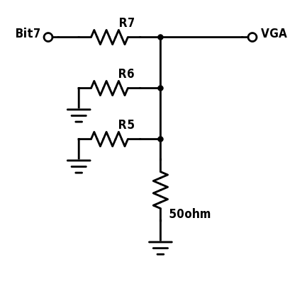
This simply means that R2 in the equation above will be replaced by R6 || R5 || 50ohm. Knowing the values that we want for each bit, and the schematic for each configuration, we can now compute the values of the resistors using superposition.
Superposition: The voltage at the VGA port for any combination of high bits from the FPGA will simply be the sum of its voltage due to each one.
This allows us to write: VVGA = V7 + V6 + V5, where these are the voltage due to Bit 7 being high while the other two are low, Bit 6 being high while the other two are low, and Bit 5 being high while the other two are low, respectively. From the truth table above, we can see that V7= .57, V6= .29, and V5= .14. The numerical computation is done below in Matlab.
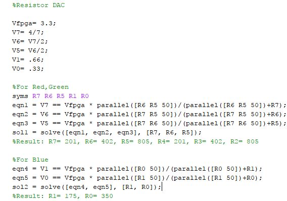
Then we found those resistor values in the bins, and soldered them onto our DAC.
Quartus
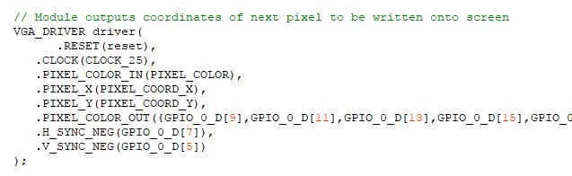
Once the DAC was finished, we could connect to the screen! We first connected the FPGA to the desktop computer USB port via cable and opened up Quartus. After downloading the project from the course website, the first step is to click File -> Open Project and select DE0_NANO.qpf from wherever you saved it. Then you can click File -> Open and select DE0_NANO.v. This is the code we will modify in the lab; the VGA_DRIVER.v file handles communication to the screen but all we need to know for now if that it provides us with the inputs PIXEL_COORD_X and PIXEL_COORD_Y and we send it the output PIXEL_COLOR.
The next step is to load this program onto the FPGA. Click Processing -> Start Compilation to compile the project, and then Tools -> Programmer. From there, you should click Hardware Setup -> Add Hardware and select the USB Blaster (It may require install). Then you can return to the programmer page, click Start, and you should see the green progress bar indicate that the board has been programmed.
The initial code was set to blink an LED and also turn the screen green. The LED was blinking, but we still needed to figure out how to wire the FPGA to the VGA connector that we built, though. To do this, we looked through the verilog file DE0_Nano.v and found where the outputs were initialized.
We could see that they were set to the odd GPIO0 pins 9-23. We found these pins by looking at the pinout diagrams in the datasheet attached here: available here and looked on the FPGA to locate GPIO0. Then we simply had to connect these pins to the VGA connector and lo and behold, we saw the green screen as well as the blinking LED!!
Modifying the Output
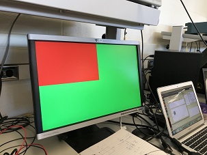
Our next step was to change the code so that we could color different quadrants on the screen. We did this by simply adding an if-statement checking the xy location of the inputs PIXEL_COORD_X and PIXEL_COORD_Y. If it was within a certain bound, we assigned one color to output PIXEL_COLOR. Otherwise, we assigned PIXEL_COLOR a different 8-bit color. We were able to verify that this worked immediately.
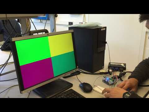
Finally, we wanted our screen to be able to respond to external inputs; we wired up the circuit below with four switches controlling the color for each of the quadrants. We had to modify the code slightly by adding a condition checking the value of these GPIO inputs in our if-statement, but after that change, this worked as well.
Acoustics Team:
- Paige
- Yonghun
- Jimmy
Goal: use an FPGA to generate a tune composed of three different frequencies. This tune will be played when the robot has indicated that it has completed searching the maze.
Materials:
- Arduino Uno
- FPGA DE0_nano
- Lab speaker
- Stereo phone jack socket
- 8-bit R2R DAC (digital-to-analog converter, datasheet here: available here )
We started by generating the simplest signal we could think of, which is a square wave. We arbitrarily chose a frequency of 440 Hz (audible frequency for humans is 20Hz - 20kHz). Using Team Alpha’s code as a guide, we programmed the FPGA with the following code:
// Local parameter
localparam CLKDIVIDER_440 = 25000000/440/2;

// Sound variables
reg square_440;
assign GPIO[0] = square_440;
reg [15:0] counter;

// Sound state machine
always @ (posedge CLOCK_25) begin
  if (counter == 0) begin
    counter    <= CLKDIVIDER_440 - 1;
    square_440 <= ~square_440;
  end
  else begin
    counter    <= counter - 1;
    square_440 <= square_440;
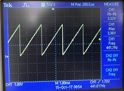
If the internal clock of the FPGA runs at 25MHz, a single cycle of a 440 Hz signal will contain 25000000/440 clock cycles and if we want to produce a square wave at this frequency, the output must toggle twice every period, or every 25000000/440/2 clock cycles. The above code counts down from this number every clock cycle and toggles the output of the GPIO pin 0 when this countdown reaches 0 and then resets.
We checked the output of this code by connected the GPIO pin to an oscilloscope and got the following result:
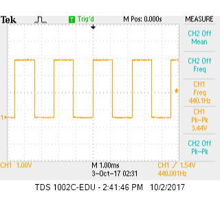
As expected, the FPGA outputs a square signal at 440 Hz. We also connected the output to the speaker so see if we could hear this signal as well.
We now want to be able to produce a more complex signal, like a sine wave. In order to do so, we first had to create a sine lookup table that Quartus could easily iterate over. We produced this table in MATLAB.
module SINE_ROM(

    input [9:0] addr,
    input clk,
    output reg [7:0] q
	);

  // Declare the ROM variable
  reg [7:0] sine[628:0];

  initial
  begin
     sine[0] <= 8'b10000000;
sine[1] <= 8'b10000001;
sine[2] <= 8'b10000010;
sine[3] <= 8'b10000011;
sine[4] <= 8'b10000101;
sine[5] <= 8'b10000110;
sine[6] <= 8'b10000111;
sine[7] <= 8'b10001000;
sine[8] <= 8'b10001010;
sine[9] <= 8'b10001011;
sine[10] <= 8'b10001100;
sine[11] <= 8'b10001110;
...				//continues assigning values from 12 to 623
sine[624] <= 8'b01111010;
sine[625] <= 8'b01111100;
sine[626] <= 8'b01111101;
sine[627] <= 8'b01111110;
sine[628] <= 8'b01111111;
  end

  // Read from requested address of ROM
  always @ (posedge clk)
  begin
    q <= sine[addr];
  end
  endmodule
We decided to represent a complete sine wave with 629 points as this would allow for a fine enough resolution without taking up too much memory. Since the DAC has 8 inputs, we are limited to outputting a minimum integer value of 0 and a maximum integer value of 2^8 - 1 = 255. The remaining part of the code converts the sine outputs to binary and prints them in a way that can be copied and pasted directly into a Quartus file.
We then created a sine ROM module in Quartus that takes two inputs:
- clk
- [0:9] addr (corresponding to the 629 points of the generated sine wave)
And one output:
- [7:0] q (8 bit output of sine wave at given address)
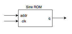
The module assigns the value of sine[addr] to q every posedge of the clk.
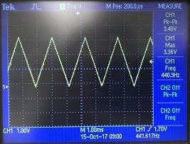
We then created an instance of this module in the DE0_NANO file and modified the square wave code. We first changed CLKDIVIDER_440 to 25MHz/440Hz/629 since this is now the number of clock cycles that we want to iterate over our sine table to produce a 440 Hz sine wave. The code creates a counter variable that is assigned the value of CLKDIVIDER_440 and counts down every clock cycle, changing the value of the addr input to the sine_ROM module when counter reaches 0. The output of the FPGA was then connected to the DAC and then to the speaker as shown by the pseudo code and module schematic below.
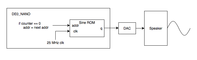
Note that q is an 8 bit signal, so we defined the output pins for the FPGA as GPIO_0_D[32:25] since the other earlier pins were already allocated for visual output to the monitor. We connected the pins using the following pinout:
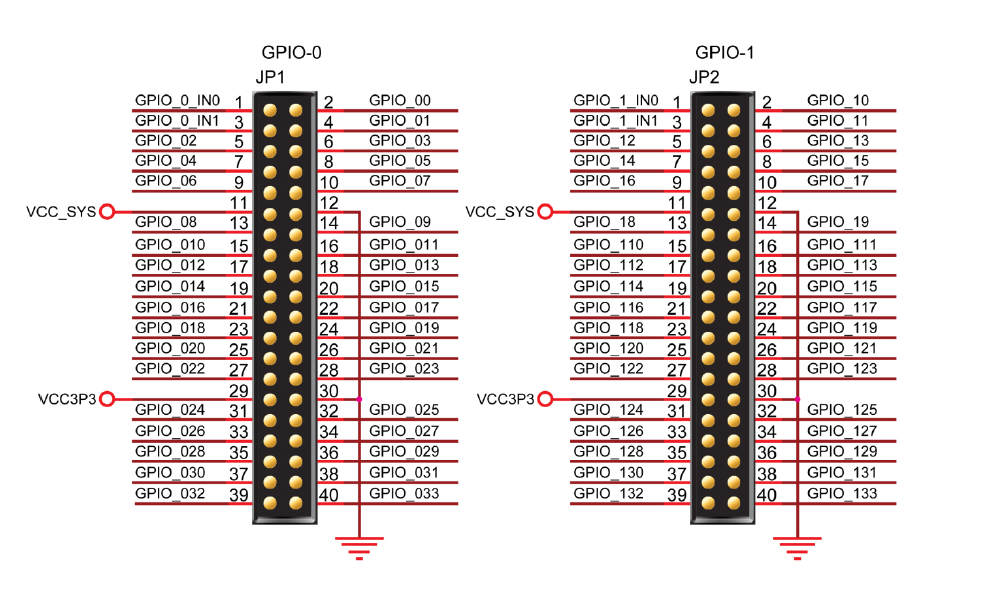
(Image from FPGA manual, found at Terasic Website)
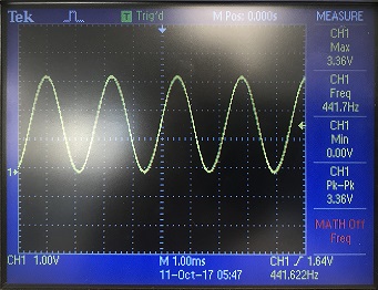
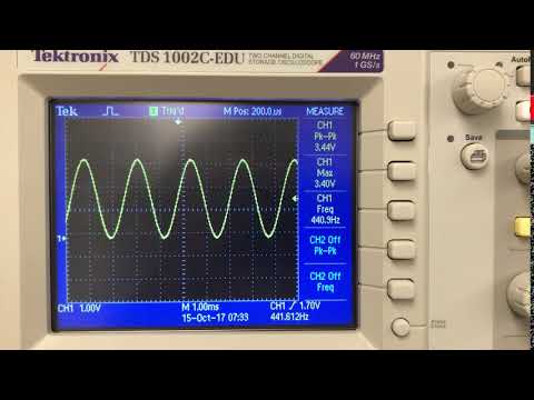
We connected the DAC output first to an oscilloscope to check if we were producing a 440Hz sine wave.
We also generated triangle and sawtooth waveforms with the same MATLAB-generated lookup tables.
Each waveform, even at the same frequency, generates different sound, confirmed by these sounds from sine wave and sawtooth wave.


We decided to use sine wave for a short tune, because it sounded softer and purer than square, triangle, or square waves (We will play the sine wave sound later!). The difference in sounds is explained by a presence of harmonics. A sine wave contains only the fundamental frequency and lacks any other harmonics, whereas the other waves experimented here have harmonics, and therefore create denser and buzzier sounds. Sawtooth wave contains both odd and even harmonics, and so it sounds denser than triangle wave that contains only odd harmonics (can you hear the difference?).
Using a sine wave signal, we then created a 3-second tune by varying the frequency three times consecutively every one second.
First, we assigned two more local CLKDIVIDER parameters for two additional frequencies (200Hz and 700Hz), produced the same way as the 440Hz one. Second, another counter register variable is created to keep track of time so that we can play a tune of the following form:
(0 – 1 second : 200Hz, 1 – 2 seconds : 440Hz, 2 – 3 seconds : 700Hz).
- NOTE: The state machine clock we use is 25MHz, and so the counter will count all the way up to three times 25 million (counting up to three seconds). Therefore, we need to assign at least 27 bits to this new counter.
And then, inside the always-block that we originally used to create a single frequency sine wave, we added the following code. This code now continuously produces the three-second tune above.
if (tone_counter == 0) begin
  CLKDIVIDER <= CLKDIVIDER_200;             //Start the tune with 200Hz
end
tone_counter <= tone_counter + 1;
if (tone_counter == ONE_SEC) begin          //At 1second mark, 440Hz will be played
  CLKDIVIDER <= CLKDIVIDER_440;
end
else if (tone_counter == 2*ONE_SEC) begin   //At 2seconds mark, 700Hz will be played
  CLKDIVIDER <= CLKDIVIDER_700;
end
else if (tone_counter == 3*ONE_SEC) begin   //At 3seconds mark, the counter goes back to 0
  CLKDIVIDER <= CLKDIVIDER_200;
  tone_counter <= 0;
end
Here’s a video of oscilloscope screen that shows three different waveforms with distinct frequencies in sequence. When the output signal is played on the speaker, this is how it sounds!
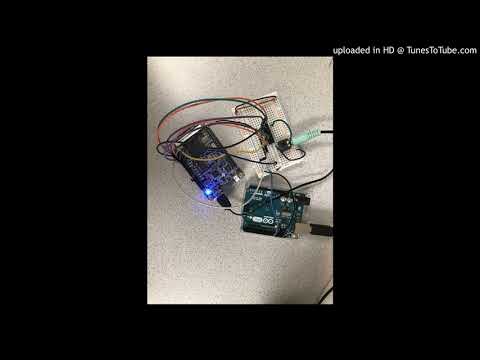
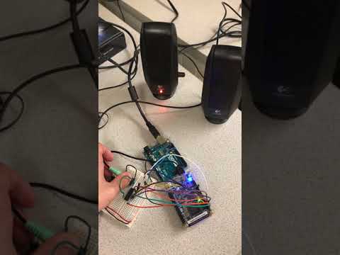
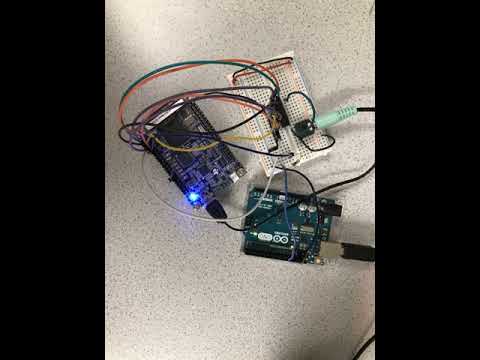
The final step is to make the FPGA play the audio only when it receives a done-signal from an external source. In our final robot design, the robot will wirelessly send this signal remotely to the FPGA when it completes mapping the maze. For now, we decided to directly send the Arduino’s digital output signal from one of its digital pins to one of GPIO pins.
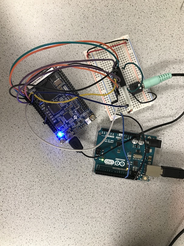
We used the following Arduino code to turn the digital signal on and off. We turned it on for three seconds, and off for four seconds. We let it run in a continuous mode to check that FPGA consistently responds to the Arduino signals.
void setup() {
  pinMode(12, OUTPUT);  //Digital pin that is connected to FPGA's GPIO pin
}

void loop() {
  // put your main code here, to runrepeatedly:
  digitalWrite(12, HIGH);
  delay(3000);  //Play audio for 3 seconds
  digitalWrite(12, LOW);
  delay(4000)   //Turn off the signal for 4 seconds
}
Subsequently, we made a simple modification on our Verilog code by putting everything inside the always-block into an if-statement checking the state of one GPIO pin connected with one of Arduino’s digital pins.
*NOTE: When the Arduino’s signal is off, the time counter must be initialized to 0. Otherwise, when the FPGA receives the signal and starts generating tunes, it might start at a different frequency.
Here’s our fully integrated code block in Verilog.
// Local parameter, Sound variables here//
...

// Count the amount of time that has passed
reg [26:0] tone_counter;

// Receive signal from an external source
assign  signal_Arduino = GPIO_0_D[24];

// Sound state machine
always @ (posedge CLOCK_25) begin
  if (signal_Arduino == 1) begin	// External signal is ON

    // Tone_counter block here //
   ...

    // Sine wave generation
	if (counter == 0) begin		// Toggle to the next point on the waveform
	  if (addr != 628) begin
	    counter <= CLKDIVIDER - 1;
	    addr <= addr + 1;
	  end
	  else begin			// End of one period of the waveform
	    counter <= CLKDIVIDER - 1;
	    addr <= 0;
	  end
	end
	else begin
	  counter <= counter - 1;
	  addr <= addr;
	end
   end
   else begin  				// External signal is OFF
      tone_counter <= 0;
   end
end

SINE_ROM sine(
  .addr(addr),
  .clk(CLOCK_25),
  .q(GPIO_0_D[32:25])
);
And finally, this is a video capturing FPGA generating 3-seconds audio tune upon receiving signal from the Arduino. The Arduino is sending a digital signal every 7 seconds (on for three seconds, and off for four seconds). If FPGA is responding to Arduino signals consistently, FPGA should play the tune and become idle for four seconds, and repeat again.